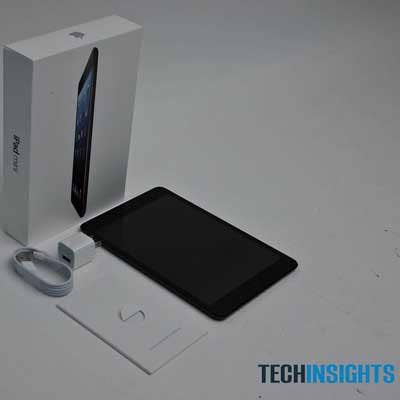
Teardown: A Look Inside Apple's iPad Mini
Inside iPad mini
For a company that's quick to litigate against Samsung for infringing on its software, Apple certainly isn't ashamed to use opponent's hardware in its devices. The latest case in point is the iPad mini, wherein three primary components are made by Samsung.
For a look inside Apple's latest device, which reportedly sold three million units in its first weekend, we turned to UBM Channel sister company UBM TechInsights for analysis from one of its patented teardowns.
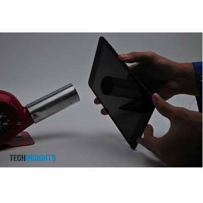
Lots Of Hot Air
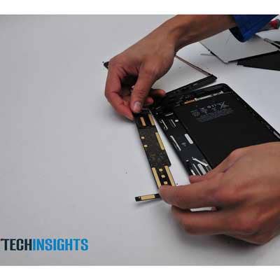
Getting inside the iPad mini will require lots of hot air. The unit's touch screen is held in place by a plastic bezel that's secured by generous portions of industrial adhesive. So break out the blow drier and concentrate the heat on one edge at a time. Once one side is heated up, slide a thin plastic card between the bezel and the aluminum unibody. Then go to work on the other sides until the bezel can be gently removed. Careful, there's a ribbon cable that connects the touch panel to the main board. Either remove it or just fold the panel out of the way (as shown).
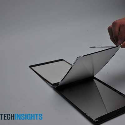
Samsung LCD
Four tiny screws secure the LCD panel to the unibody chassis, two of which are hidden beneath black flaps. Once removed, the panel lifts out easily, but it is still attached at one end by a ribbon cable. Top or bottom, the 1,024-x-768-pixel panel gives no clue as to its manufacturer. It's not until the logic board is uncovered that we learn that the circuitry in place to drive the display is made by Samsung, which also happens to supply the Retina panels for the iPad 3.
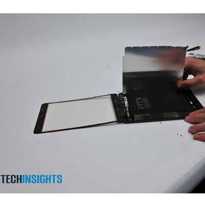
Peeling The Onion
Once the touch layer and LCD panel are removed, next comes a thin metal shield that isolates the main logic board (far left). The large black sheet is the mini's 16.3 watt-hour lithium polymer battery, which is rated to last as long as 10 hours between charges. Notice that the LCD and touch panel are two separate components. This is unlike Amazon's Kindle Fire HD and Google's Nexus 7, both of which employ fused-glass LCDs, making them a bit harder and potentially more expensive to service.
Logic In Design
Surprisingly small is the iPad mini's main logic board, which is home to all of the unit's major circuitry. Shown here from its backside, the board is held in place with adhesive, but it is best attacked after the removal of all other components. These include the power and volume buttons and the battery and stereo speakers, all of which are secured with screws and attached via ribbon cables. After heating up the underside of the case near the logic board, a spudger is helpful to pry the board from its perch.
Parts Is Parts
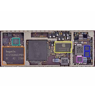
The topside of the logic board reveals all of the iPad mini's integrated circuits. The large yellow-banded area is the next-gen 32nm version of Apple's A5 SoC, which was made to Apple's specifications by Samsung. Versions of this part have been used in the original iPad 2 and the third-gen Apple TV. The large orange region is a Hynix 16-GB NAND flash unit. The green portion indicates Apple's 338S1116 audio codec, made by Cirrus Logic. Not highlighted with color is a pair of blackish circuits along the top of the right-hand section. These parts are technically labeled Apple 338S1077, but they are actually a pair of Cirrus Logic Class D Amplifiers. Apple once again uses Broadcom for most of its networking, including the BCM4334 combo chip to deliver dual-band Wi-Fi a/b/g/n single-stream MAC baseband radio, Bluetooth 4.0 + HS and an FM radio receiver (it's also in the iPhone 5).
According to an iPad mini cost analysis by iSupply, parts for the 16-GB model with Wi-Fi only cost about $188. The suggested retail price for that particular model is $329.