Nvidia Reveals Next-Gen Blackwell GPUs, Promised To 'Unlock Breakthroughs' In GenAI
At its first in-person GTC event in nearly five years, Nvidia reveals its next-gen Blackwell GPU architecture as the much-hyped successor to the AI chip giant’s Hopper platform and teases new heights in performance and efficiency with the upcoming B100, B200 and GB200 chips.
Nvidia has revealed its next-generation Blackwell GPU architecture as the much-hyped successor to the AI chip giant’s Hopper platform, claiming it will enable up to 30 times greater inference performance and consume 25 times less energy for massive AI models.
At its first in-person GTC event in nearly five years, the Santa Clara, Calif.-based company on Monday uncovered the first GPU designs to use the Blackwell architecture, which it said comes with “six transformative technologies for accelerated computing” that will “help unlock breakthroughs” in fields like generative AI and data processing, among others.
The designs are expected to arrive later this year, but the company gave no further clarification on timing. Cloud service providers expected to provide Blackwell-based instances include Amazon Web Services, Microsoft Azure, Google Cloud and Oracle Cloud Infrastructure as well as several other players, like Lambda, CoreWeave and IBM Cloud.
On the server side, Cisco Systems, Dell Technologies, Hewlett Packard Enterprise, Lenovo and Supermicro are expected to offer a plethora of Blackwell-based systems. Other OEMs supporting the GPUs include ASRock Rack, Asus, Eviden and Gigabyte.
Blackwell is Nvidia’s first architecture update for data center GPUs since generative AI applications like ChatGPT and Stable Diffusion came online in 2022 and kicked off a new wave of hype and spending on AI development, which has benefited channel partners investing in such capabilities.
The mania has paid off well so far for Nvidia, whose GPUs have been the main engines for training and running the models behind such apps. This has resulted in high and sustained demand for GPUs like the H100 and associated systems, which played a major driver in the company more than doubling its revenue last year to $60.9 billion, surpassing that of Intel.
Blackwell Designs Include B100, B200 And GB200
The first confirmed designs to use Blackwell include the B100 and the B200 GPUs, the successors to the Hopper-based H100 and H200 for x86-based systems, respectively. The B200 is expected to include greater high-bandwidth memory capacity than the B100.
The initial designs also include the GB200 Grace Blackwell Superchip, which, on a single package, connects a B200 GPU with the company’s Arm-based, 72-core Grace CPU that has previously been paired with the H200 and H100.
But whereas the Grace Hopper Superchips combine a single Grace CPU with Hopper GPU, the Grace Blackwell Superchip combines a single Grace CPU with two Blackwell GPUs, significantly increasing the performance scaling against the first generation.
It’s the GB200 where Nvidia sees Blackwell truly shining when it comes to the most demanding AI workloads, in particular massive and complex AI models called Mixture-of-Experts that combine multiple models, pushing the parameter count past 1 trillion.
In a liquid-cooled system with 18 GB200s, Nvidia said the system’s 36 Blackwell GPUs are capable of providing up to 30 times faster large language model inference performance compared to an air-cooled system with 64 H100 GPUs.
While Nvidia is promising significant advances in inference, energy efficiency and cost reductions, the energy required for the most powerful configurations of Blackwell is going up too. The company said Blackwell can be configured from 700 watts, which was Hopper’s maximum and is the maximum for the air-cooled HGX B100 form factor, to 1200 watts, which is required of the GB200 for a new, liquid-cooled rack-scale architecture.
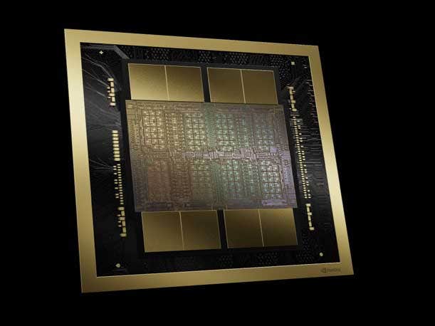
Blackwell Packs A Whopping 208 Billion Transistors
Marking a shift in Nvidia’s designs for data center GPUs, Blackwell combines “two of the largest possible dies” on a single package, according to the company. These dies are connected with a 10 TB/s chip-to-chip link, which allows them to function as a “single, unified GPU without the program behavior downsides of chiplets,” Nvidia added. This brings the GPU’s transistor count to 208 billion, a whopping 160 percent increase from the H100.
What made this design possible was a custom-built, two-reticle limit 4NP manufacturing process from foundry giant TSMC, which Nvidia called one of Blackwell’s “revolutionary technologies.”
An Nvidia spokesperson told CRN that “Blackwell is not a chiplet design,” a methodology for connecting smaller chips in a package that has been embraced by AMD for years, including for its Instinct MI300 data center GPUs, and more recently adopted by Intel for a wider range of products, including its Max Series data center GPUs.
2nd-Gen Transformer Engine Helps Blackwell Drive Faster AI
When it comes to AI performance, Blackwell GPUs are capable of performing up to 20 petaflops, which amounts to 20 quadrillion calculations per second, according to Ian Buck, vice president of hyperscale and high-performance computing at Nvidia.
This was measured using a new numerical format called four-bit floating point, or FP4 for short, that is lower in precision than the FP8 format that Blackwell’s predecessor, Hopper, introduced and used to deliver 4 petaflops in each H100.
Buck said FP4 allows Blackwell to deliver twice the amount of compute and bandwidth compared to Hopper when using FP8, and it also doubles the size of an AI model that can fit on a single GPU.
“Getting down to that level of fine granularity is a miracle in itself,” Buck said in a briefing.
This was made possible by Blackwell’s second-generation Transformer Engine, which was introduced in Hopper to accelerate models based on the transformer architecture that dominates the AI world today, such as large language models and diffusion models.
As originally designed, the Transformer Engine “tracks the accuracy of every layer of every tensor” computing unit in the GPU, according to Buck. As the GPU trains a model, the engine will “constantly monitor the ranges of every layer and adapt to stay within the bounds of the numerical precision to get the best performance,” he added.
Called one of Blackwell’s “six revolutionary technologies,” the second generation of the engine can take monitoring even granular through “micro tensor scaling,” which allows the engine to look at the “individual elements within the tensor,” Buck said.
What also helps Blackwell reach 20 petaflops in a single GPU is Nvidia’s TensorRT-LLM open-source software library, which the company launched last year to double large language model inference in an H100, and the NeMo Megatron framework for training such models.
5th-Gen NVLink Enables High-Speed Link Between 576 GPUs
Another significant technology upgrade for Blackwell touted by Nvidia is the fifth generation of the NVLink chip-to-chip interconnect that allows GPUs to communicate with each other.
The new generation enables bidirectional throughput per GPU to reach 1.8 TB/s, double the 900 TB/s that Hopper enabled with fourth-gen NVLink.
It also substantially increases the number of GPUs that can communicate with each other at these speeds, enabling “seamless high-speed communication” among a maximum of 576 GPUs. This is a big step up from the 256-GPU maximum support that was possible with NVLink in Hopper.
Buck said this solves a growing bottleneck for large clusters of GPU running massive AI models, like a 1.8-trillion-parameter Mixture-of-Experts model that contains multiple models working together to perform complex functions and deliver better responses.
“If you run a model like GPT[-4], which at 1.8 trillion parameters [is a] Mixture-of-Experts [model], you can spend up to 60 percent of your time communicating the data, and only 40 percent of the time doing computing,” Buck said of a scenario with Nvidia’s Hopper-based GPUs.
Blackwell’s Other Upgrades Include RAS Engine, Confidential Computing
The other major technology upgrades for Blackwell include:
- A dedicated RAS engine for reliability, availability and serviceability features. These sorts of features have traditionally been found in server CPUs like Intel’s Xeon chips. Nvidia’s take on RAS also includes AI-based preventative maintenance features at the chip level to reduce downtime for massive deployments.
- Advanced confidential computing capabilities that “protect AI models and customer data without compromising performance.” These capabilities include support for “new native interface encryption protocols.”
- A dedicated decompression engine that accelerates database queries for data analytics and data science applications, which Nvidia called out as growing targets for GPUs.
Blackwell To Power New DGX Systems, GB200 NVL72 Rack Systems
Nvidia is announcing two new flavors of DGX systems with Blackwell GPUs:
- The DGX B200, an air-cooled design that pairs B200 GPUs with x86 CPUs. This system is available in a DGX SuperPod cluster.
- The DGX GB200, a liquid cooled design that uses GB200 Grace Hopper GPUs. Eight of these systems make up a DGX SuperPod cluster, giving it a total of 288 Grace CPUs, 576 B200 GPUs and 240TB of fast memory. This enables the DGX SuperPod to deliver 11.5 exaflops, or quadrillion calculations per second, of FP4 computing.
The GB200-based SuperPod is made using a new version of the rack-scale architecture Nvidia introduced with AWS last year to power large generative AI applications.
Called the GB200 NVL72, it’s a “multi-node, liquid-cooled, rack-scale system for the most compute-intensive workloads,” according to Nvidia, and it contains 36 GB200 Grace Blackwell Superchips as well as the company’s BlueField-3 data processing units (DPUs).
These DPUs are meant “to enable cloud network acceleration, composable storage, zero-trust security and GPU compute elasticity in hyperscale AI clouds,” the company said.
The GB200 NVL72 systems will become the basis of the infrastructure for Blackwell-based instances offered by Microsoft Azure, AWS, Google Cloud, and Oracle Cloud Infrastructure, the latter three of which will offer Nvidia’s DGX Cloud service on top of the systems.
Nvidia plans to enable OEMs and other partners build their own Blackwell-based systems with the HGX server board, which links eight B100 or B200 GPUs. The company has not yet announced plans to offer Blackwell GPUs in PCIe cards for standard servers.
Nvidia Reveals Quantum-X800 InfiniBand, Spectrum-X800 Ethernet Platforms
To enable high-bandwidth connections between these systems, Nvidia announced two new high-speed network platforms that deliver speeds of up to 800 GB/s: the Quantum-X800 InfiniBand platform and the Spectrum-X800 platform.
Nvidia said the Quantum-X800, which includes the Quantum 3400 switch and ConnectX-8 SuperNIC, provides five times higher bandwidth capacity and offers a nine-fold increase for in-network computing, which comes out to 14.4 teraflops.
The Spectrum-X800, on the other hand, “optimizes network performance, facilitating faster processing, analysis and execution of AI workloads,” according to Nvidia. This results in expedited “development, deployment and time to market of AI solutions,” the company said.