Nvidia Unveils 7nm Ampere A100 GPU To Unify Training, Inference
'The Ampere server could either be eight GPUs working together for training, or it could be 56 GPUs made for inference,' Nvidia CEO Jensen Huang says of the chipmaker's game changing A100 GPU. 'The economics, the value proposition is really off the charts.'
Nvidia said its newly revealed data center GPU, the A100, will "revolutionize" artificial intelligence by unifying training and inference into one architecture that can outperform the chipmaker’s V100 and T4 several times over.
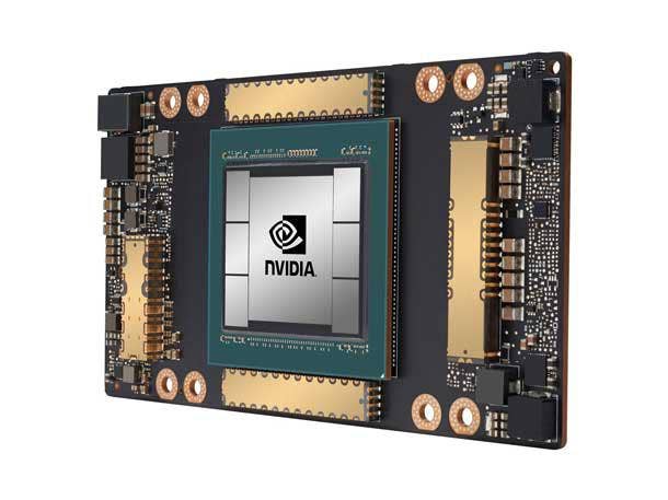
Based on the company’s new 7-nanometer Ampere GPU architecture, the A100 provides "massive flexibility" unlike any GPU the company has released before, thanks to its ability to partition into as many as seven distinct GPU inferences, Nvidia revealed during its virtual GPU Technology Conference Thursday. Alternatively, the A100 can link with seven other units to act as one giant GPU.
[Related: Nvidia's 5 Biggest GTC 2020 Announcements: From A100 To SmartNICs]
In a pre-briefing with journalists, Nvidia CEO and founder Jensen Huang said the A100 will create a tectonic shift in the economics of spinning up new data centers for AI inference and training because of the GPU’s ability to scale up and scale out at any given time.
"The Ampere server could either be eight GPUs working together for training, or it could be 56 GPUs made for inference. And so all of the overhead of additional memory and CPUs and power supplies and all that stuff of 56 servers basically collapsed into one, the economics, the value proposition is really off the charts," he said. "And that's the thing that's really exciting."
In an example given by the company, Nvidia said five DGX A100 systems – a new AI server appliance that comes with eight A100 GPUs – could provide the same amount of training and inference work as 50 V100-based DGX-1 systems and 600 CPU systems at a tenth of the cost and a twentieth of the power.
One major reason Nvidia said it can pull this off is the A100 can perform single-precision floating point math (FP32) for training workloads and eight-bit integer math (INT8) for inference 20 times faster than the V100 GPU that came out in 2017. The company said the A100 is 2.5 times faster for double-precision floating point math (FP64) for high-performance computing workloads.
Nvidia said it has made five technological breakthroughs to achieve what it said is the largest generational leap in performance across all eight generations of its GPU.
For one, the A100 contains more than 54 billion transistors on a 826 mm2 die, making what it said is the largest 7nm processor. This is made possible by to the Ampere architecture’s use of the TSMC’s 7nm manufacturing process that is also used by AMD’s Zen 2 processors.
The A100 also uses Nvidia’s new third-generation Tensor Cores that comes with a new TF32 For AI format, which enables single-precision floating point acceleration thanks to its ability to compress the number of bits needed to complete math equations. The Tensor Cores also support double-precision floating point for the first time, enabling such math problems to be solved faster.
In addition, the new Tensor Cores use a new efficiency technique called structural sparsity that takes advantage of the spark nature of AI math to speed up the execution of calculations by two times. The technique supports TF32, FP16, BFLOAT16, INT8 and INT4 formats.
Another breakthrough is the A100’s multi-instance GPU capability, allowing the GPU to be partitioned in as many as seven separate GPU instances that can perform work in parallel. This is similar to the capabilities offered by Nvidia’s vComputeServer software, except no virtualization is required.
To enable faster GPU-to-GPU communication within servers, Nvidia’s new third-generation NVLink interconnect enables 4.8 TB per second in bi-direction bandwidth and 600 GB per second in GPU-to-GPU bandwidth. This, combined with 200 Gbps Mellanox interconnects, gives servers improved throughput so that they can act more effectively as one large GPU for training massive AI models.
With the A100’s ability to perform inference and training workloads faster than Nvidia's T4 and V100 GPUs and within the same package, the idea is that organizations can be much more flexible and increase utilization with their data centers, buying up A100s to initially perform training and then direct the GPUs to do inference once the models have been trained.
"It's going to unify that infrastructure into something much more flexible, much more fungible and increase the utility makes it a lot easier to predict how much capacity you need," Huang said.
The A100 comes with 3,456 FP64 CUDA Cores, 6,912 FP32 CUDA Cores, 432 Tensor Cores, 108 streaming multiprocessors and 40 GB of GPU memory within a 400-watt power envelope.
With the A100 already in full production, Nvidia is taking the GPU to market in multiple ways: with the eight-GPU DGX A100 deep learning system that will cost $200,000, with the HGX A100 server building block meant to help OEMs and system builders make their own A100 systems and with the EGX A100 that combines an A100 with a Mellanox SmartNIC for edge computing, among other things.
OEM partners expected to release A100-based servers include Atos, Dell Technologies, Fujitsu, Gigabyte, H3C, Hewlett Packard Enterprise, Inspur, Lenovo, Quanta and Supermicro. Several cloud service providers are also expected to spin up A100-based instances, including Alibaba Cloud, Amazon Web Services, Baidu Cloud, Google Cloud and Tencent Cloud.