5 Things To Know About Intel’s Game-Changing IDM 2.0 Strategy
Intel is making a $20 billion manufacturing expansion in the U.S. while also increasing use of external foundries as part of a ‘major evolution’ in its manufacturing model, which CEO Pat Gelsinger says will result in greater chip capacity and a return to ‘unquestioned leadership.’
Better Performance, Supply At A ‘Superior Cost Structure’
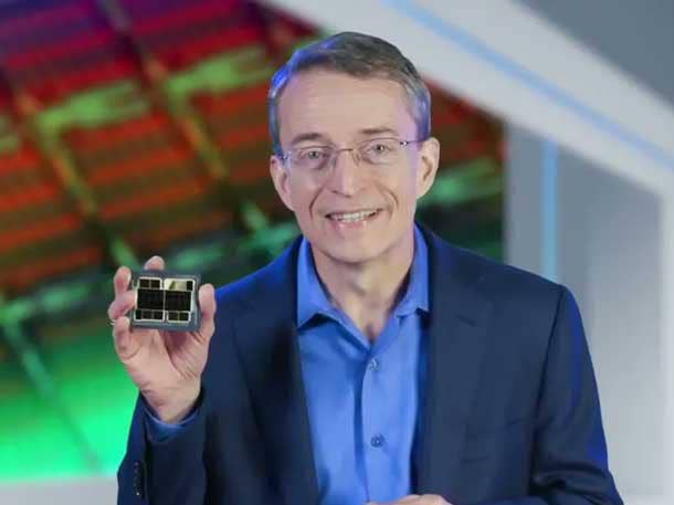
Intel CEO Pat Gelsinger on Tuesday said the company will return to “unquestioned leadership” with its newly revealed “IDM 2.0” strategy that will “significantly” expand the company’s manufacturing capacity and dramatically change the way it makes chips.
While the new strategy consists of three key initiatives, there are many moving parts in what Gelsinger called a “major evolution” in Intel’s integrated device manufacturing model, where the company produces the chips it designs.
[Related: Partners: AMD EPYC Milan Widens Gap Over Intel, Builds Trust]
With the IDM 2.0 strategy, the Santa Clara, Calif.-based company will build new manufacturing fabs, expand its use of external foundries like TSMC to make chips and launch its own foundry services business, which will manufacture chips designed by other companies like Qualcomm.
“Our IDM 2.0 plans will put us on a path to restore process performance leadership and build on our leadership packaging technologies, delivering our customers leadership products in every category that we participate in, ensure superior capacity and supply resilience with flexibility leveraging our internal and external capacity, all with a superior cost structure,” Gelsinger said in Intel’s Tuesday webcast.
What follows are five important things to know about Intel’s IDM 2.0 strategy, from its manufacturing expansion plans in the U.S. and across the world to how it plans to use external foundries to create competitive, next-generation processors.

Intel’s $20B U.S. Manufacturing Expansion Will Create More Capacity
While Intel is expanding its use of external foundries for future products, the company is also committing roughly $20 billion to create two new manufacturing fabs in Arizona.
Gelsinger said the new fabs will be used to produce Intel products, but it will also be used to produce chips designed by other companies as part of the new Intel Foundry Services business, which will provide “committed capacity” for foundry customers.
The CEO promised that the new fabs, in combination with Intel’s plan to expand outsourcing to external foundries, will “ensure superior capacity and supply resilience” and give the company more flexibility in using external or internal manufacturing capacity to product parts.
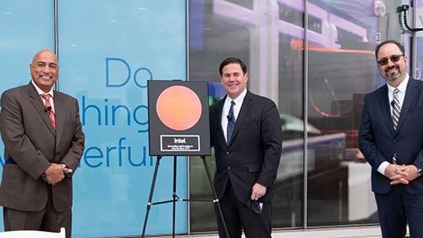
The two new fabs will be built on Intel’s Ocotillo campus in Chandler, Ariz., and they will create more than 3,000 permanent “high-tech, high-wage” jobs as well as more than 3,000 construction jobs and 15,000 “long-term” jobs in the state, according to Gelsinger. Planning and construction for the two fabs will begin this year, he added.
Gelsinger said the two new fabs will be capable of using extreme ultraviolet lithography, or EUV, an advanced chip fabrication method that means they will be capable of producing chips with Intel’s 7-nanometer process technology and more advanced processes in the future.
The increased fab capability will help Intel develop “unquestioned leadership” for supply chain, manufacturing and process technology, according to Gelsinger.
Intel is working with the state of Arizona and President Joe Biden’s administration on incentives to support the new factories, Gelsinger said. But when asked if federal and state incentives were necessary for the fabs, he said they were not. However, he added, government incentives will help accelerate Intel’s manufacturing plans and counter the large incentives provided to foundries in Asia.
“We want incentives, we want investments, because it is the right thing for them to accelerate manufacturing and this imbalance of the global supply chain,” Gelsinger said.
He added that Intel is also competing for a contract with the U.S. Department of Defense to build a “domestic, commercial foundry that will also meet the security needs of the U.S. government.”

Intel Will Expand Use Of Foundries Like TSMC To Produce Chips
While Intel plans to continue to build the majority of its products using its own fabs, Gelsinger said the company will ramp up use of external foundries like TSMC and Samsung to ensure that the chipmaker can “deliver the best products in every category that we participate in.”
Gelsinger said Intel’s use of external foundries isn’t new: The company has already been using foundries to make chips for communications, connectivity, graphics and chipsets.
But the new IDM 2.0 strategy means that Intel will turn to external foundries for top products the company had previously manufactured in-house, according to Gelsinger. That includes CPUs for servers and PCs coming out in 2023 that will rely on TSMC.
Gelsinger said Intel is increasing its use of foundries across the board: not just TSMC and Samsung but also GlobalFoundries and UMC.
“This will provide us with the increased flexibility and scale we need to optimize our roadmaps for cost, performance, schedule and supply, giving us a unique competitive advantage,” he said.
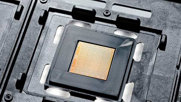
The foundries will be used to support Intel’s new modular approach to building chips that will make use of “tiles,” which can be made using different manufacturing processes, internal and external, based on cost, supply and performance considerations, Gelsinger said. Intel will use its Foveros 3D packaging technology to stack the tiles vertically for upcoming processors.
One upcoming Intel product that will rely on internal and external manufacturing processes is the company’s previously announced Ponte Vecchio XPU, which will integrate 47 tiles in a package using Foveros and Intel’s Embedded Multi-die Interconnect Bridge technology to deliver a petaflop of compute power for high-performance computing applications. That’s equivalent to the performance of a large supercomputer IBM deployed 13 years ago, Gelsinger noted.
This speaks to a larger industry transition as customers‘ needs and workloads diversify and grow in complexity,” he said. “The world will move from system-on-a-chip to system-on-package, and Intel’s unquestioned leadership and packaging technologies becomes even more valuable. Being able to expertly construct the best products using the best technologies is a critical differentiator for us and one that delivers enormous value for our customers.”
Intel Will Return To ‘Unquestioned Leadership’ For CPUs In 3-4 Years
As part of the IDM 2.0 strategy, Gelsinger vowed that Intel will return to “unquestioned leadership” for its CPU products by 2024 or 2025 while restoring the company’s “tick-tock” model that was abandoned during its 10-nanometer struggles.
Intel previously used the tick-tock model to bring new advances to every product generation, with alternating enhances in manufacturing process and architecture.
For years, this approach resulted in a predictable shrink of the processors’ transistors every two or so years, which brought new performance and efficiency benefits. But when the company struggled to deliver a viable 10nm node on schedule, it ditched the tick-tock model in 2016 to focus on improvements in architecture and elsewhere.
But with the new IDM 2.0 strategy, Gelsinger said Intel will re-establish that “tick-tock discipline.”
Beyond its CPU plans, Gelsinger said Intel will also provide “unquestioned leadership” for AI, graphics and networking technologies as part of Intel’s multi-architecture “XPU” product strategy.
“Those areas are ones that we have solid positions, but trust me, we‘re going to accelerate the investments that we have in those areas,” he said.
Gelsinger admitted that Intel’s 10nm issues created a “domino effect” and contributed to the company pushing out its timeline for next-generation 7nm products.
Intel’s 7nm work was also complicated by the company’s original plan to limit its use of extreme ultraviolet (EUV) lithography as an advanced fabrication method, but the company has since fully adopted it, Gelsinger said, and Intel’s 7nm process is now “on a good course.”
The company expects to “tape in” the 7nm compute tile of Intel’s 2023 client CPU, Meteor Lake, in the second quarter of this year, according to Gelsinger. Meteor Lake will also include tiles using other manufacturing processes, all of which will be integrated using Intel’s Foveros 3D packaging technology.
“Our technology teams are moving rapidly through process maturity, and as they do, our confidence in 7nm health and competitiveness is accelerating,” he said.
Intel Foundry Services, A New Biz For Creating Other Companies’ Chips
In addition to ramping up its use of external foundries, Intel is also launching a new standalone business to provide foundry services to companies making their own chips.
The new business is called Intel Foundry Services, and Gelsinger said it will “become a major provider” of chip manufacturing capabilities for companies in the United States and Europe. He cited cloud service providers and Apple as examples of companies Intel would like to gain as foundry customers. Apple, Amazon Web Services, Microsoft and Google Cloud are all now designing their own chips, which have created new threats for Intel’s traditional processor businesses.
“Imagine if you were a major cloud service provider saying, ‘boy, I have tens of millions of cores that are running, and now I can optimize them for my business and add some of my stuff and maybe take out some things that I don‘t utilize?’ This is a powerful strategy, and we believe that now is the time for Intel Foundry Services,” Gelsinger said.
Gelsinger said Intel Foundry Services could lead to the company collaborating with competitors like Qualcomm, which is among the companies that have expressed early support for the new business. Other companies that are supporting the establishment of Intel Foundry Services include Amazon, Cisco, Ericsson, Google, IBM, Microsoft and SiFive.
Between Intel’s increasing use of foundries and the creation of its own foundry business, the company will increasingly cooperate with its competitors and vise-versa.
“This is clearly a co-opetition story,” Gelsinger said, “and one that, by managing our business judiciously, by creating more business opportunities, leveraging our world-class IP portfolio, we see IDM 2.0 as a unique strategy for Intel, and one that the world needs right now.”
Intel will offer foundry customers its IP for x86 cores, graphics, AI and interconnect, and the business will also support customers who have designs based on Arm and RISC-V architectures, according to Gelsinger. He added that foundry customers will also have access to Intel’s chip packaging technologies like Foveros and Embedded Multi-die Interconnect Bridge as well “leading” process technologies.
Intel Foundry Services will be led by Randhir Thakur, a company executive who joined intel in 2017 after previously serving in multiple leadership roles at Applied Materials, a Santa Clara, Calif.-based provider of engineering solutions for chip manufacturing.
Gelsinger said Intel believes the total addressable market for foundry services will be $100 billion by 2025, “with most of the growth coming from leading-edge computing, which is our expertise.” The establishment of more foundry capacity in the U.S. will help balance out the heavy concentration of foundries in Asia, he added.
Intel Enters New Collaboration With IBM For Next-Gen Chip Technologies
To support Intel’s IDM 2.0 strategy, the company is beginning a new research collaboration with IBM to create next-generation logic and packaging technologies for processors.
Gelsinger said the new collaboration will “accelerate the velocity of packaging and process innovations into the future” — a sentiment that was shared by IBM CEO Arvind Krishna in Intel’s webcast.
“This represents an important milestone in the world of technology,” Krishna said. “By bringing together two of the best semiconductor research organizations in the world, we will greatly accelerate innovations in the semiconductor industry.”
In a press release, IBM said the collaboration “will enhance the competitiveness of the U.S. semiconductor manufacturing industry, support key U.S. government initiatives, and help deliver significant economic value.”
Krishna said IBM has a “long tradition of creating game-changing innovations in the industry” and that the new collaboration will provide a boost to 5G, hybrid cloud, AI and other technologies.
“The future of technology has to be built on a foundation of deep industry collaboration,” he said.
IBM is expected to release its 7-nanometer Power10 processor for the company’s Power systems in the second half of this year. The Power10 will be IBM’s first commercialized processor made using Samsung’s 7nm manufacturing node as part of a long-term strategic partnership.