6 Big Announcements From Intel Architecture Day 2020
From multiple discrete GPUs shipping within the next year to a historical intranode enhancement for Tiger Lake, the semiconductor giant made several new disclosures to show that it is investing in next-generation design methodologies to help it overcome manufacturing issues.
'A Major Engineering And Architecture Transformation'
Intel is looking to give customers and partners confidence in its next-generation products with a new “transistor-resilient design” approach that will impact everything from its forthcoming Tiger Lake mobile processors to multiple discrete GPU products it plans to release within the next year.
The Santa Clara, Calif.-based company made several new product and technology disclosures at its Intel Architecture Day pre-briefing event on Tuesday, including news that discrete GPUs for laptops and servers will ship later this year and that it has delivered the largest single intranode enhancement with the new version of its 10-nanometer process that will power Tiger Lake.
[Related: Partners: Intel Still Strong Despite 7nm Delays, AMD Gains]
With the disclosures, the company is hoping to show that it is investing in next-generation design methodologies that will help it overcome any issues in the future with internal manufacturing capabilities, which recently prompted the company to delay the launch of 7nm products by six months.
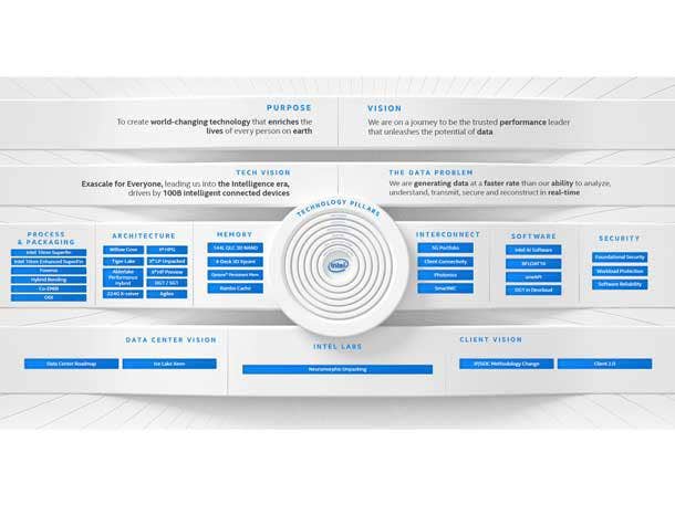
“We at Intel are going through a major engineering and architecture transformation that sets us up for the next decade and reimagines our design methodology, architecture and the way we solve problems for our users and customers,” said Raja Koduri, an AMD veteran who is now Intel‘s chief architect and who leads the Architecture, Graphics and Software Group.
What follows are six big announcements from Intel Architecture Day 2020, made public Thursday, that range from Intel‘s big discrete GPU and Tiger Lake news to its 10nm desktop processor plans and how it plans to take a building-block approach for client processors in the future.

Intel's First Discrete GPUs For Servers And Laptops To Launch This Year
Intel seems intent on delivering on the promise it made in 2018 when the company said its first discrete GPUs would come out in 2020. At this week‘s Intel Architecture Day, the company said it will launch its DG1 GPU for laptops and a newly disclosed SG1 GPU for servers this year.
Revealed at CES 2020 at the beginning of the year, DG1 is in production and on track to ship later this year, according to Intel, but the company did not say how many laptops will use it.
SG1, which combines the power of four DG1 GPUs, is based on Xe-LP, Intel‘s low-power GPU microarchitecture, like the DG1, and it and will come in a small form factor for servers targeting low-latency, high-density Android cloud gaming and video streaming. The company said SG1 will enter production soon and ship later this year.
Intel also revealed two other GPU types, one based on the company‘s Xe high-performance GPU microarchitecture for data centers and another based on the newly disclosed Xe high-performance gaming GPU microarchitecture for desktop PCs.
The company said its first Xe-HP GPU for servers—which will ship next year and is already sampling with customers—represent the “industry‘s first multi-tiled, highly scalable, high-performance architecture” that will provide GPU scalability, artificial intelligence optimization and media performance. With its multi-tile nature, the Xe-HP GPU will come in three configurations—one tile, two tiles and four titles— the latter two of which Intel said will make it function like a multi-core GPU.
The company said Xe-HP can also deliver on the compute side, providing the most single-precision floating-point, or FP32, performance on a single GPU package. The company said it can also deliver high performance for media workloads and demonstrated a single Xe-HP tile transcoding 10 full streams of 4K video at 60 frames per second and multiple Xe-HP tiles.
“The single-precision FP32 performance numbers of over 40 teraflops is already impressive and respectable, considering that the best GPU in the market today is the 20 teraflops range,” said Raja Koduri, Intel‘s chief architect and head of the Architecture, Graphics and Software Group.
Intel‘s Xe-HPG GPU for desktop PCs is also set to start shipping next year, and it will feature a new memory subsystem based on GDDR6 and hardware-accelerated ray tracing. The company said the Xe-HPG GPU will incorporate “building blocks” from Xe-LP for efficiency, Xe-HP for scalability and Xe-HPC for optimized compute frequency. Xe-HPC is the basis for the company’s previously announced Ponte Vecchio GPU for high-performance computing and AI workloads.

Intel Teases Purpose-Built 'Client 2.0' Processors With 'Mix And Match' Building Blocks
While many of Intel‘s new disclosures focused on products coming within the next year or two, the company also teased a more long-term change in how the company is designing next-generation chips for desktops and laptops in the future.
The company calls this new approach to client processor design “Client 2.0,” and it will focus on the creation of ”purpose-built” processors for different user types, like gamers, content creators and commercial users. This approach will be made possible by mixing and matching different silicon functions and IPs as building blocks—for things like graphics, compute and I/O—to optimize for different experiences, which is a major departure from Intel‘s traditional monolithic chip approach.
Brijesh Tripathi, vice president and chief technology officer for Intel‘s Client Computing Group, said Client 2.0 will allow a much quicker development time than it takes for monolithic and multi-die chips, which is made possible in part by the fact that the individual IP building blocks can be reused for different products at a much greater rate than its multi-die design methodology.
“Overall, Client 2.0 is about delivering winning products at an annual cadence,” he said.
Tripathi said the company plans to share more details of its Client 2.0 plans in the future.
“We‘ve been working on this for quite some time,” he said. ”In a world where customers demand extremely rich experiences for every use case, we have changed the way we think about our construction tools and methodology. Our purpose has changed from building monolithic general-purpose SoCs to building scalable, purpose-built devices to provide rich user experience.”
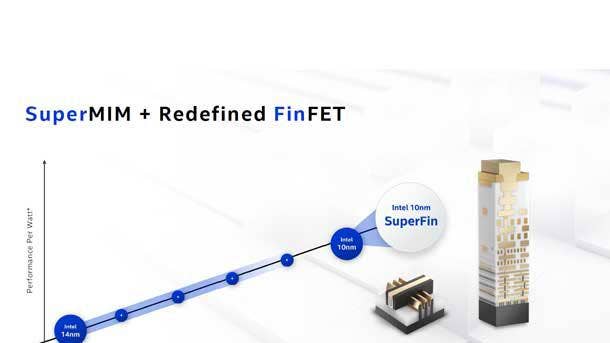
Intel Reveals 10nm SuperFin, 'Largest Single Intranode Enhancement'
Intel is taking a new approach to intranode enhancements for its products and getting rid of the plus sign that has been used for previous intranode enhancements like 14nm+++, the latest version of the company‘s 14-nanometer process used for processors like the Comet Lake H chips.
Headlining the new approach is Intel‘s first improvement of its 10nm process, called 10nm SuperFin, which the company said is the “largest single intranode enhancement in its history,” comparable to a full-node transition performancewise.
Ruth Brain, an Intel Fellow and director of interconnect technology and integration., said SuperFin is a redefining of the 3D FinFET transistors Intel introduced over a decade ago that have served as the foundation for the company‘s 14nm and 10nm products to date.
“The era of getting massive performance boost from simply shrinking transistor features is behind us,” she said.
10nm SuperFin, which serves as the basis for Intel‘s forthcoming Tiger Lake mobile processors, combines the company’s enhanced FinFET transistors with a new super metal-insulator-metal capacitor to drive performance and efficiency improvements in a variety of ways.
The improvements include enhanced epitaxial growth of crystal structures and an additional gate pitch option to drive higher current through the transistor‘s channels. 10nm SuperFin also includes an improved gate process for higher channel mobility, a novel thin barrier to reduce electrical resistance by 30 percent and improve interconnect performance, as well as a five-fold increase in capacitance, which results in a reduction in voltage troop that “dramatically” improves performance.
“This is an industry-first technology that far exceeds the current capabilities of other manufacturers,” Brain said.

Intel Promises 'More Than Generational Performance Leap' With Tiger Lake
Intel promises a “more than generational performance leap” as well as massive improvements in graphical and artificial intelligence performance with its upcoming Tiger Lake mobile processors, which are expected to go into more than 50 laptop designs for the holiday season.
The Tiger Lake processors use the company‘s new Willow Cove CPU microarchitecture that is based on the new 10nm SuperFin process and, for the first time, the company’s Xe low-power graphics microarchitecture for its integrated graphics.
Willow Cove improves upon Intel‘s Sunny Cove microarchitecture—which was the basis for last year’s 10nm Ice Lake mobile processors—by significantly increasing the frequency, made possible by optimizing the entire range of the voltage-to-frequency curve.
“We were able to deliver a greater than generational improvement performance by not only dramatically lowering the voltage at which Willow Cove achieves its operating frequencies versus Sunny Cove, but we were also able to extend the range,” said Boyd S. Phelps, vice president of the Client Engineering Group and general manager of the Client and Core Development Group.
“Willow Cove is better, faster and more efficient, enabling generational CPU gains in not only thermal dynamic-limited performance, but also unconstrained performance across the board,” he added.
Willow Cove also includes a redesigned caching architecture that allows it to have a 1.25-MB midlevel cache. The core also uses a new hardware-based security feature to fight against malware, called Intel Control-Flow Enforcement Technology.
Tiger Lake‘s Xe graphics will feature up to 96 execution units to deliver 1,536 flops per clock, and it will also have a significant improvement in performance-per-watt over Ice Lake’s integrated graphics. The company said users can expect “outstanding performance across a breadth of games, including previous unachievable gameplay on some AAA titles” in an ultra-thin laptop form factor. The company demonstrated a clear improvement in frames per second for multiple games running on Tiger Lake’s Xe graphics over the chipmaker’s previous Gen11 integrated graphics.
Tiger Lake‘s other features and improvements include a doubling of the coherent fabric bandwidth, enabling roughly 86 GBps in memory bandwidth; RAM support for LP4x-4267, DDR4-3200 and LP5-5400 RAM; a new version of the Gaussian Network Accelerator for low-power neural inferencing that lowers CPU utilization by roughly 20 percent; and autonomous dynamic voltage frequency scaling for power management. Tiger Lake also has integrated support for Thunderbolt 4.0, USB 4.0 and PCIe 4.0.

Intel's First 10nm Desktop CPUs, Alder Lake, Will Use Hybrid Architecture
Intel‘s long-waited 10-nanometer processors for desktops, code-named Alder Lake, won’t arrive until the second half of 2021, but the company revealed one major detail a year ahead of launch: They will use Intel’s hybrid architecture approach that was first seen in this year’s Lakefield mobile chips.
Whereas Lakefield processors consisted of one high-performance Sunny Cove core and four low-power Tremont Cores, Alder Lake will use the successors for the respective core types—Golden Cove for high performance and Gracemont for low power—to optimize performance-per-watt.
Koduri said the company is working on a next-generation hardware-guided scheduler that will optimize Alder Lake processors to squeeze every ounce of performance out of each core. Beyond delivering great performance, Alder Lake will also be Intel‘s “best performance-per-watt architecture,” he added.
“While Lakefield was tuned for battery life, in Alder Lake, we have advanced the hybrid architectures significantly with a focus on performance,” he said.

Intel Provides More Details For Ice Lake, Sapphire Rapids Server CPUs
With Intel set to begin making initial shipments of its Ice Lake server processors by the end of the year, the company provided more details on the next-generation Xeon chips as well as its successor, Sapphire Rapids, which is set to begin shipping for production in the second half of 2021.
The company said Ice Lake, which will be its first 10nm server processor line, will bring a significant improvement in performance for both throughput and responsiveness for “all workloads.” The processors will include total memory encryption, a new instruction set for accelerating crypto processing as well as support for PCIe 4.0 and eight memory channels. The company is also planning Xeon D variants for network and storage as well as IoT variants for the Ice Lake lineup.
As for Sapphire Rapids, Intel said the next-generation Xeon Scalable line will use an enhanced version of its SuperFin technology that is being introduced with its forthcoming Tiger Lake mobile processors. The processors will support Compute Express Link 1.1, DDR5 memory, PCIe 5.0 and new built-in acceleration for artificial intelligence called Advanced Matrix Extensions.
“We have the silicon in our labs and are excited about sampling it to customers soon,” said Sailesh Kottapalli, an Intel Senior Fellow in the Intel Architecture, Graphics and Software Group and chief architect for data center processor architecture.